
Target Materials
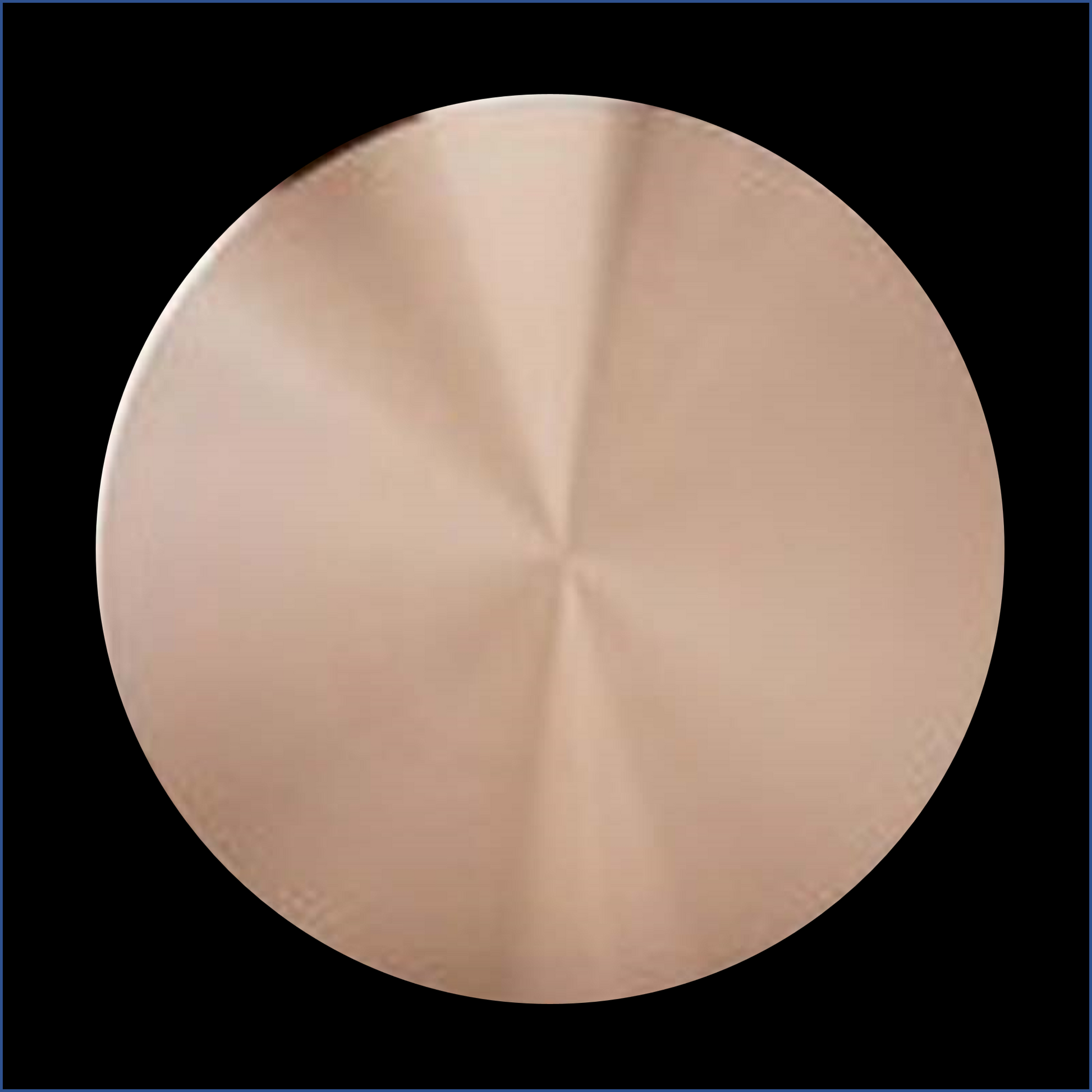
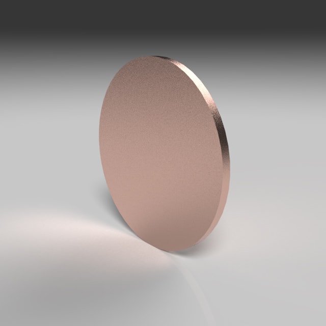
Copper (Cu) Sputtering Target
Copper (Cu) Sputtering Target
Couldn't load pickup availability
| Material | Copper |
| Formula | Cu |
| Purity | 99.999% |
| Typical Substrates | Si, GaAs, InP |
| Related Materials | Au, Ag, Al, Ti, Cr, Ni, Zn |
Copper (Cu) thin films are a versatile material used in a variety of research and commercial applications due to their unique properties. Copper thin films are used in electronics, optoelectronics, and biomedical devices, and have been used for decades in many different types of products. A few examples include transistors, solar cells, sensors, and electrical wiring. Copper thin films are also used in the development of optical waveguides due to their light-guiding properties. In electronics, copper thin films are used as electrical conductor in various components and circuits. Copper thin films are also used in optoelectronic devices, such as lasers and light-emitting diodes (LEDs), which rely on the properties of copper thin films to control the flow of light. In biomedical applications, copper thin films are used to create high-resolution images of tissues and organs in order to better understand the structure and function of the human body.
What is the Typical Conductivity of Copper Thin Films
Copper thin films have excellent electrical conductivity, making them an ideal material for use in electronics and optoelectronics. The electrical conductivity of a copper thin film is typically between 4 -6 x10⁶ S/m. This is significantly higher than the conductivity of other thin film materials, such as gold (Au) and silver (Ag). The excellent conductivity of copper thin films makes them highly desirable for use in a range of applications, from transistors to waveguides.
How are Copper Thin Films Usually Deposited?
Thin Films Copper thin films are typically deposited using physical vapor deposition (PVD) techniques such as sputtering and electron assisted evaporation. These methods involve the application of a high-energy beam of particles, typically electrons or ions, to the surface of a substrate to cause the release of material from a target. The released material then deposits onto the substrate, forming a thin film of copper. Other PVD techniques, such as pulsed laser deposition (PLD), are also used to deposit copper thin films. In PLD, a laser beam is used to vaporize the target material, which is then deposited onto the substrate.
What Substrates Support Epitaxial Growth of Copper Thin Films
Epitaxial growth is a process by which a thin film is grown layer-by-layer on a substrate material. Copper thin films can be epitaxially grown on a variety of substrate materials, including silicon (Si), gallium arsenide (GaAs), and indium phosphide (InP), sapphire, silicon, and silicon carbide. These materials are often chosen due to their high thermal conductivity, which is important for the growth of quality copper thin films.
What Substrates Support Growth of Quality Polycrystalline Copper Thin Films?
Polycrystalline copper thin films can be grown on a variety of substrate materials, including glass and silicon. These materials are chosen due to their ability to support the formation of crystalline structures at temperatures that are relatively low compared to other materials. Copper thin films can also be grown on other materials, such as gallium arsenide, aluminum nitride, and zinc oxide.
Research Papers on the Deposition of Quality Copper Thin Films
- H. Y. Yang, “Deposition of copper thin films by physical vapor deposition,” Thin Solid Films, vol. 467, pp. 1–10, 2004.
- S. A. Kulkarni, “Pulsed laser deposition of copper thin films,” Applied Surface Science, vol. 255, pp. 6192–6198, 2009.
- D. G. Grigoriev, “Sputtering deposition of copper thin films,” Materials Science and Engineering: B, vol. 131, pp. 154–164, 2006.
- M. B. Stankovich, “Pulsed laser deposition of copper thin films,” Applied Physics A, vol. 78, pp. 851–855, 2004.
- T. A. Gireesh, “Growth and characterization of copper thin films by pulsed laser deposition,” Journal of Materials Science, vol. 44, pp. 1277–1287, 2009.
- M. Abou-Ras et al. “Sputtering of Copper Thin Films on Glass Substrates at Low Temperature” (2010).
- A. Alam et al. “Pulsed Laser Deposition of Copper Thin Films from Copper Chloride Precursors” (2005).
- Abe et al. “Structure and Properties of Copper Thin Films Deposited by Reactive Sputtering” (2007).
- Y. Kim et al. “Atomic Layer Deposition of Copper Thin Films for High Performance Transistors” (2008).
- T. Ly et al. “Deposition of Copper Thin Films by Direct Current Magnetron Sputtering” (2009).
Some Interesting Facts about Copper
- Copper is one of the first metals to have been used by humans.
- Copper has a high thermal and electrical conductivity, making it an ideal material for use in electronics and optoelectronics.
- Copper is an essential trace element for human health, and is found in a variety of foods.
Materials
Materials
Shipping & Returns
Shipping & Returns
Dimensions
Dimensions
Care Instructions
Care Instructions


-
Free Shipping
Wherever you are, get free shipping on orders from Target Materials
-
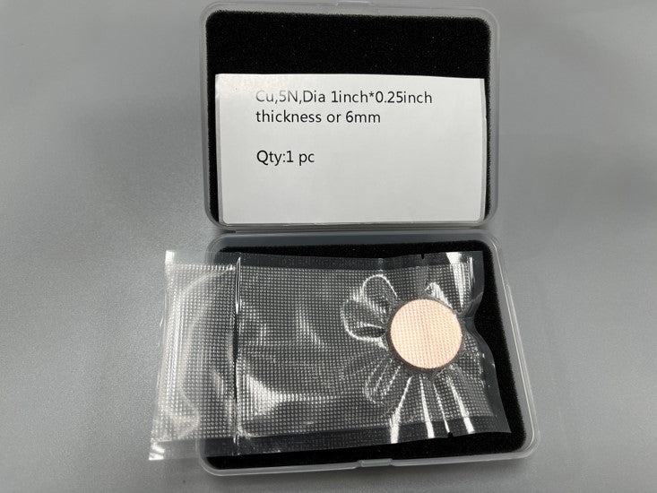
High Quality Packaging
All our targets are vacuum packed, sealed and protected so they arrive with you exactly how they left from us.