


Target Materials
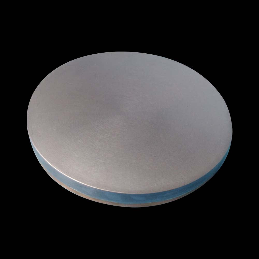
Molybdenum Disulfide MoS2 Sputtering Target
Molybdenum Disulfide MoS2 Sputtering Target
Couldn't load pickup availability
| Material | Molybdemum Disulfide |
| Formula | MoS2 |
| Purity | 99.99% |
| Typical Substrates | |
| Related Materials | MoSe2, WS2, WSe2, MoTe2, and MoS3 |
Molybdenum disulfide (MoS2) is a layered compound of molybdenum and sulfur. It is a member of the transition metal dichalcogenide (TMD) family and is one of the most studied two-dimensional materials due to its unique electrical, optical, and mechanical properties. MoS2 has a layered structure with a hexagonal lattice in which molybdenum atoms form a plane of hexagons, and sulfur atoms are arranged above and below the molybdenum plane. This structure gives MoS2 excellent electrical properties, making it a good material for thin film deposition.
What substrates are MoS2 thin films typically deposited on?
Epitaxial films of MoS2 can be grown on a variety of different substrates, including sapphire, silicon carbide (SiC), and gallium nitride (GaN). The most commonly used substrates are SiC and GaN, as they have a lattice constant similar to MoS2, making them well-suited for the growth of highly ordered, epitaxial films.
High-quality polycrystalline films of MoS2 can be grown on a variety of substrates, including sapphire, silicon, and gold. The substrate chosen will depend on the desired properties of the film, as well as the desired deposition technique. For example, sapphire is well-suited for sputtering deposition, while silicon is better suited for chemical vapor deposition. Gold is a suitable substrate for both techniques.
What are the typical properties of MoS2 in thin film?
MoS2 thin films are used in a variety of applications, including electronic devices, optoelectronic devices, protective coatings, and biocompatible materials. The typical properties of MoS2 in thin film form depend on the deposition method and processing conditions. MoS2 thin films exhibit excellent electrical and thermal conductivity, as well as good transparency in the visible light spectrum. The electrical conductivity of MoS2 thin films can be adjusted by doping with other materials such as boron, phosphorous, and nitrogen.
What are the typical deposition conditions for MoS2 thin films by sputtering?
The typical deposition conditions for MoS2 thin films by sputtering include a substrate temperature of 150-200°C, a deposition pressure of 0.3-0.5 mTorr, and a sputtering power of 10-50 W. The sputtering target is typically positioned at a distance of 5-10 cm from the substrate.
What are the typical deposition conditions for MoS2 thin films by PLD?
The typical deposition conditions for MoS2 thin films by pulsed laser deposition include a substrate temperature of 500-900°C.
Research papers of interest on MoS2
1. Zhang, X., et al. (2015). “Large-Scale Synthesis of High-Quality Monolayer MoS2 Layers and Their Adaptability for Field Effect Transistors.” ACS Nano, 9(11), pp. 11018–11026.
2. Wang, C., et al. (2014). “High-performance and solution-processed MoS2 transistors.” Nature Nanotechnology, 9(9), pp. 672–677.
3. Kappera, R., et al. (2014). “Growth and Characterization of MoS2 Thin Films by Pulsed Laser Deposition.” ACS Applied Materials & Interfaces, 6(15), pp. 12383–12390.
4. Jariwala, D., et al. (2013). “Atomically Thin MoS2: A New Direct-Gap Semiconductor.” ACS Nano, 7(4), pp. 3223–3230.
5. Bao, Q., et al. (2012). “Graphene-Based Ultracapacitors.” Nano Letters, 12(6), pp. 4632–4638.
6. “Structure and Properties of Molybdenum Disulfide Thin Films Grown by Pulsed Laser Deposition", by Jing Wang et al., Applied Surface Science, 2018.
7. “Molybdenum Disulfide Thin Films with High Electrical Conductivity Grown by Pulsed Laser Deposition", by Zhiqiang Wang et al., ACS Applied Materials & Interfaces, 2017.
8. “High-Performance and Transparent MoS2 Thin-Film Transistors”, by M. Kaempgen et al., Nature Nanotechnology, 2012.
9. “Fabrication of Molybdenum Disulfide Thin Films by Magnetron Sputtering”, by J. Zhang et al., ACS Applied Materials & Interfaces, 2013.
Materials
Materials
Shipping & Returns
Shipping & Returns
Dimensions
Dimensions
Care Instructions
Care Instructions
-
Free Shipping
Wherever you are, get free shipping on orders from Target Materials
-
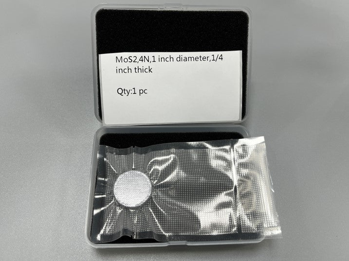
High Quality Packaging
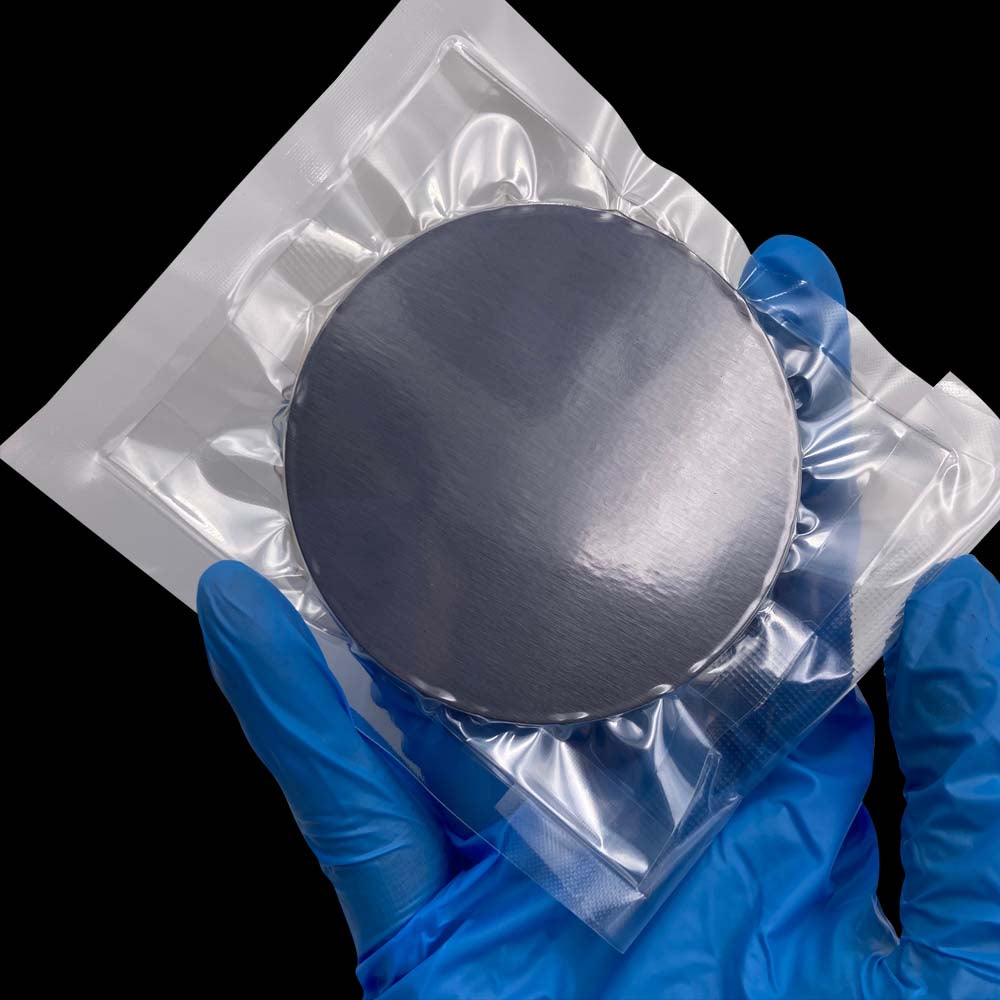
All our targets are vacuum packed, sealed and protected so they arrive with you exactly how they left from us.