


Target Materials
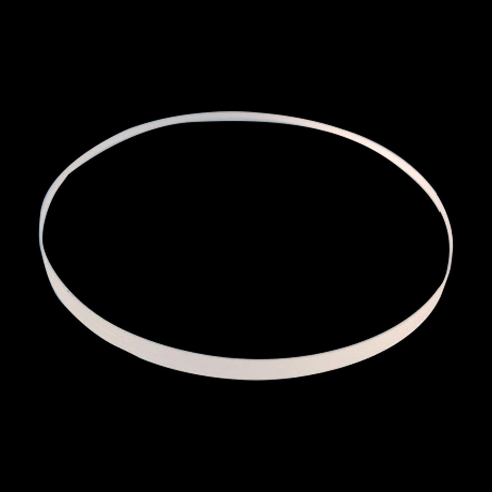
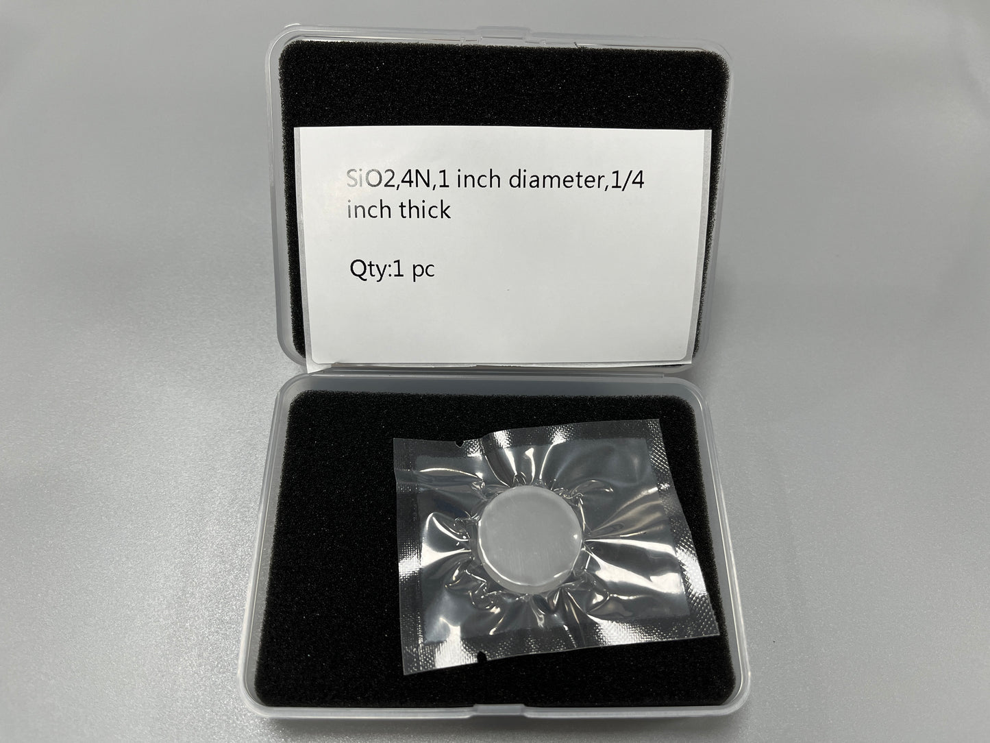
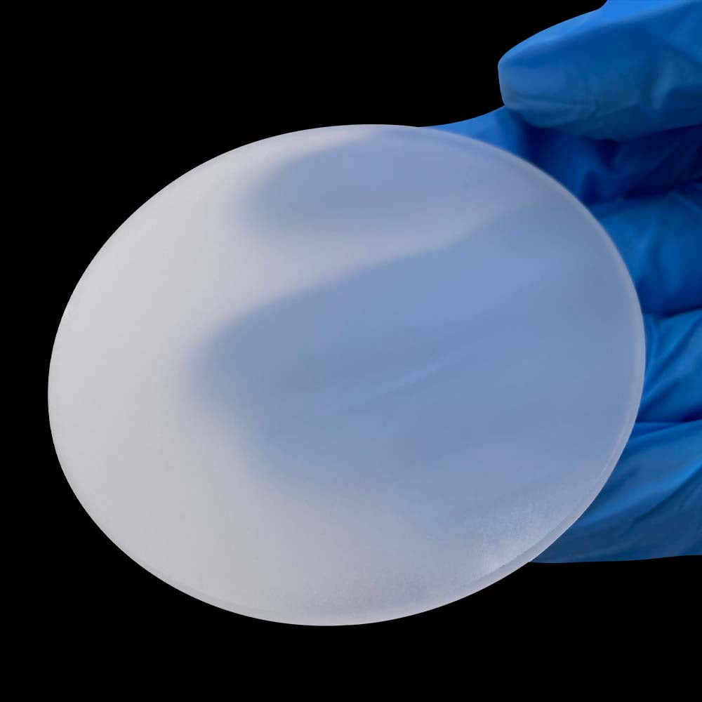
Silicon Dioxide (SiO2) Sputtering Target
Silicon Dioxide (SiO2) Sputtering Target
Couldn't load pickup availability
| Material | Silicon Dioxide, Silica |
| Formula | SiO2 |
| Purity | 99.99% |
| Typical Substrates | Si, GaAs, Al, GaN |
| Related Materials | Si3N4, ZrO2, AlN, TiO2, ZnO and Ta2O5 |
SiO2 thin films are used in a variety of devices, such as solar cells, semiconductors, optical devices, and displays. SiO2 thin films are also used in medical applications, such as drug delivery, implants, and implants for neural stimulation. SiO2 thin films are also used in the manufacture of optical filters, and in the fabrication of optical lenses. SiO2 thin films are also used in the fabrication of data storage media, such as CDs and DVDs.
What is the Typical Resistivity of SiO2 Thin Films?
The typical resistivity of SiO2 thin films is typically between 10^5 and 10^15 ohm-cm. This is dependent on the film thickness and deposition conditions, such as the deposition temperature, pressure, and the type of deposition technique (sputtering, chemical vapor deposition, etc.). The resistivity of SiO2 thin films can be increased by increasing the deposition temperature, using higher oxygen pressures, and using thicker films.
Can SiO2 be deposited by DC Sputtering?
As a dielectric material SiO2 is more suited to RF sputtering rather than DC sputtering due to charge build up during growth.
Common Deposition Conditions for Silicon Dioxide Films by RF Sputtering
The power used for sputtering is typically between 0.2 kW and 3 kW. The pressure is typically between 0.001 mbar and 0.1 mbar. The substrate bias is typically between -50 V and +50 V. The substrate temperature is typically between 20°C and 100°C.
What Substrates Permit Epitaxial Films of SiO2
Epitaxial films of SiO2 can be deposited on substrates such as silicon (Si), gallium arsenide (GaAs), aluminum (Al), and gallium nitride (GaN).
Other Techniques to Deposit Silicon Dioxide Thin Films
Other techniques that can be used to deposit SiO2 thin films include chemical vapor deposition (CVD), atomic layer deposition (ALD), and pulsed laser deposition (PLD).
Materials
Materials
Shipping & Returns
Shipping & Returns
Dimensions
Dimensions
Care Instructions
Care Instructions
-
Free Shipping
Wherever you are, get free shipping on orders from Target Materials
-
High Quality Packaging
All our targets are vacuum packed, sealed and protected so they arrive with you exactly how they left from us.