


Target Materials
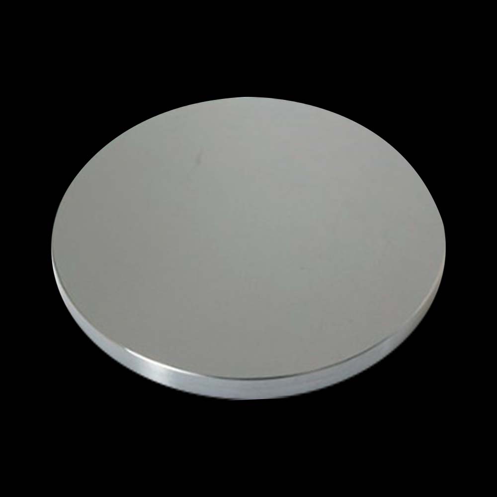
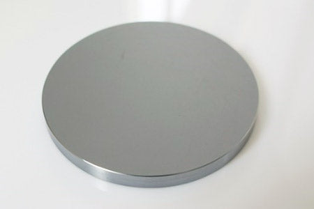
Silicon (Si) Sputtering Target
Silicon (Si) Sputtering Target
Couldn't load pickup availability
| Material | Silicon |
| Formula | Si |
| Purity | 99.999% |
| Typical Substrates | Si, GaAs, Ge |
| Related Materials | Ge, GaAs, AlN, ZnO BN |
Silicon (Si) is the most commonly used material in the semiconductor industry. It is used in many different industries including consumer electronics, automotive, aerospace and defence, medical equipment, and renewable energy. Silicon is a very versatile material, which is why it has become so popular. It can be used to create many different electrical components including transistors, diodes, and integrated circuits. It is also used in photovoltaic cells and other renewable energy technologies. Silicon is also used in many different types of thin film devices including photonics, optoelectronics, and sensors. Thin film devices are made by depositing thin layers of silicon on a substrate using various deposition techniques.
What is the Typical Conductivity of Si Thin Films?
The resistivity of silicon thin films is typically between 10^3 to 10^6 ohm.cm. This range is dependent on the deposition conditions used to create the film, which controls the microstruture as well as the intrinsic and extrinsic doping concentration. Silicon thin films can be either doped or undoped, and the level of doping affects the electrical properties of the material. Undoped silicon thin films have a low conductivity, while doped films have higher conductivities.
Doping in Si Thin Films
The conductivity of silicon thin films can be controlled by controlling the intrinsic dopants during the thin film growth process. The type of dopants used affects the conductivity of the silicon thin film. For example, boron is typically used as a p-type dopant, while phosphorus is used as an n-type dopant. The addition of these dopants allows for the control of the conductivity of the silicon film.
Depositing Dielectric SiO2 Thin Films on Si Thin Films
SiO2 is often deposited on top of Si layers to form electrically insulating / dielectric layers. The SiO2 layer acts as an insulating barrier and prevents current from flowing between the two layers. This is a common process used in the manufacture of integrated circuits.
Common Deposition Conditions for Silicon Films by DC Sputtering
DC sputtering is one of the most common techniques used to deposit silicon thin films. The pressure used for DC sputtering is typically between 0.1 and 10 mTorr, with higher pressure resulting in higher deposition rates. The substrate temperature used for DC sputtering is typically between room temperature and 400°C, with higher temperature resulting in higher deposition rates.
What Substrates Support Epitaxial Films of Si?
Epitaxial Si thin films can be deposited on a variety of substrates, including germanium, and gallium arsenide as well as homoepitaxy on silicon. The substrate must also be clean and free from contaminants in order for the epitaxial growth to be successful.
What Substrates Support Polycrystalline Si Films?
Quality polycrystalline Si thin films can be deposited on a variety of substrates, including silicon, glass, quartz, and alumina. The substrate must also be able to withstand high temperatures, as the deposition process requires temperatures of up to 500°C.
Give 5 Other Thin Film Materials Related to Si
Other thin film materials related to Si include germanium, gallium arsenide, aluminum nitride, boron nitride, and zinc oxide. These materials are often used in combination with Si to create devices such as transistors, diodes, and integrated circuits.
Materials
Materials
Shipping & Returns
Shipping & Returns
Dimensions
Dimensions
Care Instructions
Care Instructions
-
Free Shipping
Wherever you are, get free shipping on orders from Target Materials
-
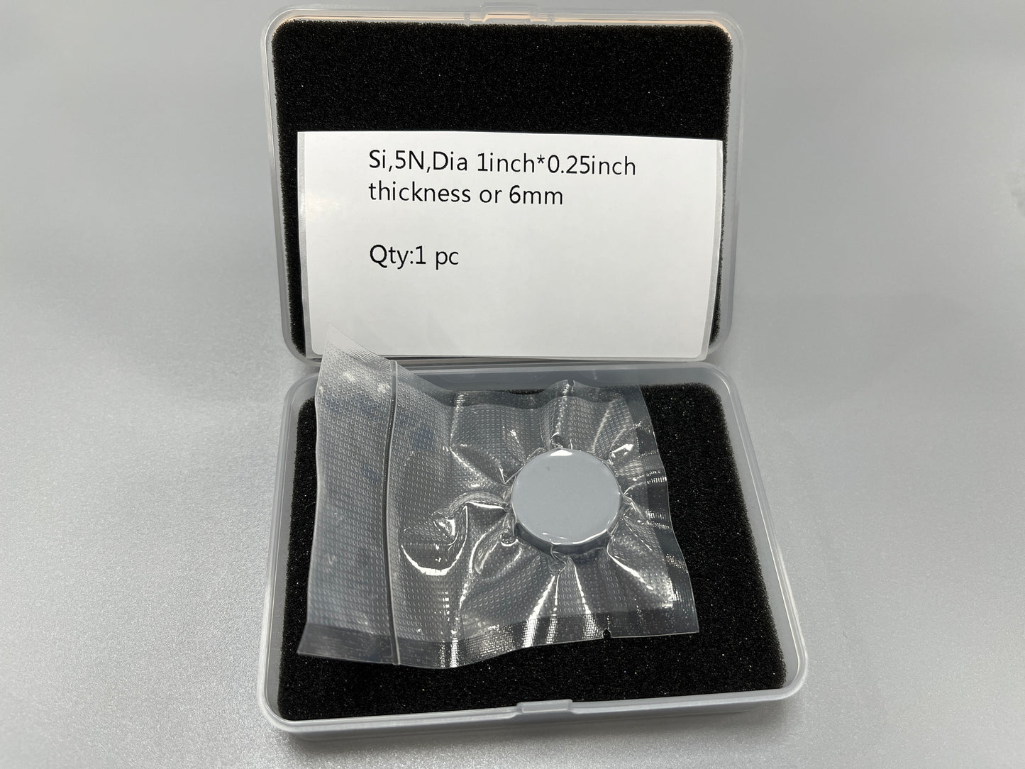
High Quality Packaging
All our targets are vacuum packed, sealed and protected so they arrive with you exactly how they left from us.