


Target Materials
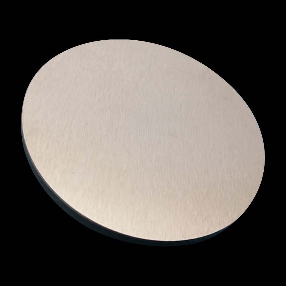
Tungsten (W) Sputtering Target
Tungsten (W) Sputtering Target
Regular price
$80.00 USD
Regular price
Sale price
$80.00 USD
Unit price
per
Shipping calculated at checkout.
Couldn't load pickup availability
| Material | Tungsten |
| Formula | W |
| Purity | 99.999% |
| Typical Substrates | Si, GaAs, AlN, glass, quartz |
| Related Materials | Ta, Ti, Mo, Co, Ni |
Tungsten (W) thin films are widely used in research and commercial applications due to their excellent electrical and thermal properties. These films offer a wide range of possibilities for the fabrication of electronic, optoelectronic and microelectronic devices. Tungsten thin films are commonly used in semiconductors, microelectronic components, and optical coatings, as well as in other applications such as high-temperature and corrosion-resistant coatings.
Tungsten thin films are used in various electronic components such as transistors, resistors, capacitors, and diodes. In addition, these films are used in the fabrication of microelectronic devices such as microprocessors and memory chips, as well as in the production of optical components like lasers and displays. Tungsten thin films are also used in the fabrication of medical devices, including sensors, implants, and prostheses. Furthermore, tungsten thin films are used in the aerospace, automotive, and nuclear industries, where they provide protection against radiation and extreme temperatures.
How Are Tungsten Thin Films Usually Deposited?
Tungsten (W) thin films are usually deposited using physical vapor deposition (PVD) techniques such as sputtering, electron beam evaporation, and pulsed laser deposition. These techniques involve the deposition of tungsten atoms onto a substrate in order to form a thin film. Other deposition techniques such as chemical vapor deposition (CVD) or atomic layer deposition (ALD) can also be used to deposit tungsten thin films.
What Substrates Support Epitaxial Growth of Tungsten Thin Films?
Tungsten (W) thin films can be grown epitaxially on various substrates, including single-crystal silicon, gallium arsenide, and aluminum nitride. Silicon is the most commonly used substrate for epitaxial growth of tungsten thin films, due to its low cost and wide availability. Other substrates such as gallium arsenide and aluminum nitride can also be used for epitaxial growth of tungsten thin films, although these materials are more expensive and less widely available.
What Substrates Support Growth of Quality Polycrystalline W Thin Films
Polycrystalline tungsten thin films can be grown on a variety of substrates, including silicon, quartz, glass, and sapphire.
Other Thin Film Materials Related to W
Some other thin film materials related to tungsten (W) are tantalum, titanium, molybdenum, cobalt, and nickel. These materials have similar properties to tungsten and are often used in similar applications. For example, tantalum and titanium thin films are commonly used in semiconductor devices, while molybdenum, cobalt, and nickel thin films are often used in components requiring high temperature and corrosion resistance.
Research Papers Which on the Deposition of Quality Tungsten Thin Films.
1. “High quality tungsten (W) thin films by RF magnetron sputtering”, Y. Yamamoto et al., Thin Solid Films, 516, pp. 7500-7504 (2008).
2. “Structure and properties of tungsten thin films deposited by magnetron sputtering”, D.S.S. Rao et al., Vacuum, 60, pp. 119-122 (2002).
3. “Pulsed laser deposition of tungsten thin films on Si(100)”, S.K. Singh et al., Vacuum, 70, pp. 7-13 (2002).
4. “Optical properties and microstructure of tungsten thin films deposited by pulsed laser deposition”, A.L. Xie et al., Thin Solid Films, 514, pp. 495-501 (2006).
5. “Nanostructured tungsten (W) thin films by pulsed laser deposition”, M. Srinivasan et al., Thin Solid Films, 520, pp. 6595-6600 (2012).
Interesting Facts About Tungsten
1. Tungsten (W) was discovered by Carl Wilhelm Scheele in 1781 and was initially called wolfram.
2. Tungsten is a refractory metal with the highest melting point of any metal (3422 °C).
3. Tungsten is used in a variety of applications, including electronics, metallurgy, optics, and medical devices.
4. Tungsten is used in the filament of incandescent light bulbs and in the electrodes of arc lamps.
5. Tungsten is a dense, heavy metal and is about twice as dense as lead.
Materials
Materials
Shipping & Returns
Shipping & Returns
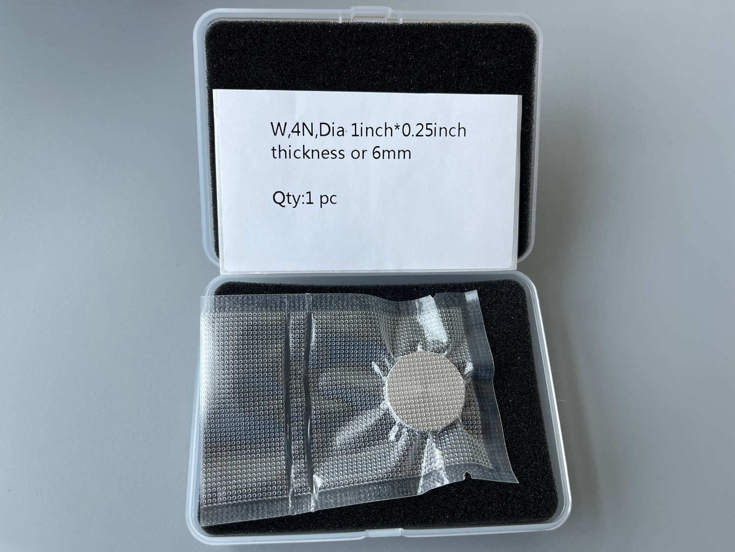
Dimensions
Dimensions
Care Instructions
Care Instructions
-
Free Shipping
Wherever you are, get free shipping on orders from Target Materials
-
High Quality Packaging
All our targets are vacuum packed, sealed and protected so they arrive with you exactly how they left from us.