


Target Materials
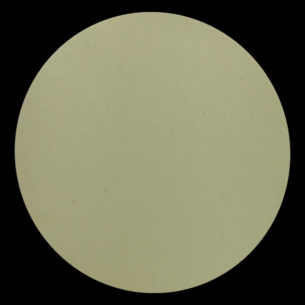
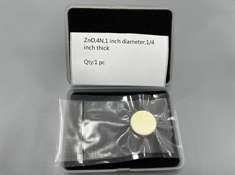
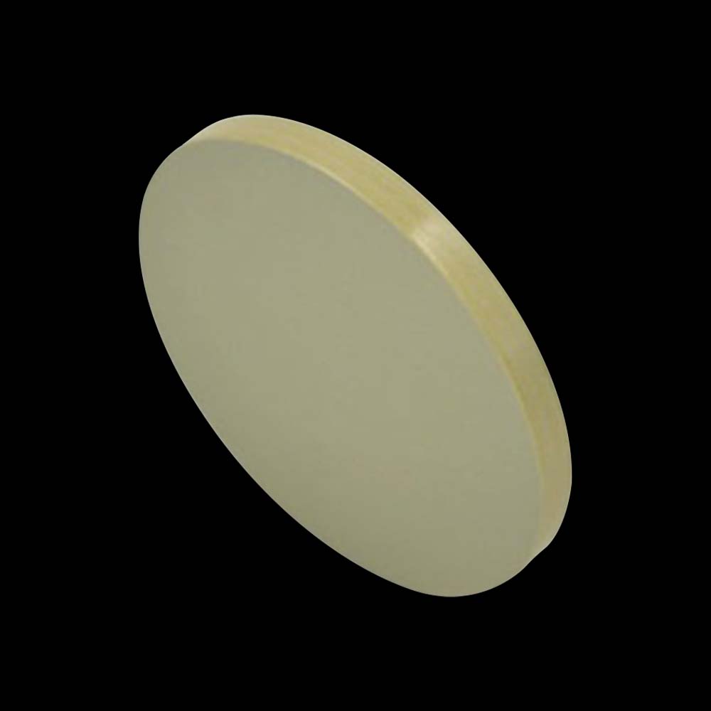
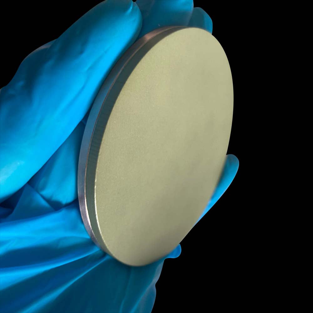
Zinc Oxide ZnO PLD Target
Zinc Oxide ZnO PLD Target
Couldn't load pickup availability
| Material | Zinc Oxide |
| Formula | ZnO |
| Purity | 99.99% |
| Typical Substrates | Al2O3, Glass, Quartz, Sapphire, Polymers, Silicon and Silicon Dioxide |
| Related Materials | ITO, TiO2, Al2O3, In2O3 |
Zinc Oxide Targets for Pulsed Laser Deposition
Zinc Oxide (ZnO) is a wide bandgap material with high transparency in the visible spectrum, high electron mobility and can be doped with various elements making it a highly studied materials for use in a variety of optoelectronic devices such as light emitting diodes, solar cells, and sensors.
It is universally agreed that a ZnO target should be dense (>90 %) which reduces particulate inclusion in deposited films.
Zn-rich Surface of PLD targets
After exposure to repeated laser pulses, changes in stoichiometry of the ZnO target have been observed, with the surface becoming zinc rich after irradiation [Claeyssens
et al.] It was found by XPS that after hitting the target with a few hundred pulses results in a 5 fold decrease in the oxygen: zinc ratio in the near surface region, The explanation for this is the redeposition of Zn onto the target. Subsequently films deposited are zinc rich meaning that they must be compensated for by reaction with background oxygen in the chamber during deposition.
PLD ZnO films deposited under 1 mTorr will normally have lots of defects as a result of low oxygen and may appear grey. Films deposited with a background oxygen pressure 5-25 mTorr are typically oxygen deficient and will have high electrical conductivity as a result. Films deposited 50 mTorr and above will typically be close to 1:1 oxygen stoichiometric.
As the oxygen deficiency occurs within the first few hundred pulsed (which is in line with typical pre-ablation run in the chamber to clean the target surface, it is advised to compensate with oxygen in the chamber rather than continually sanding back the target.
Crystal Structure of ZnO
ZnO has a wurtzite crystal structure and is a direct bandgap material with a bandgap energy of 3.37 eV.
Optoelectric Properties of ZnO
The optoelectric properties of ZnO make it an ideal choice for use in a variety of optoelectronic devices. These properties include high transparency in the visible spectrum, high electron mobility, and a wide bandgap. These properties make ZnO suitable for use in devices such as light emitting diodes, solar cells, and sensors.
Typical Substrates for Zinc Oxide Thin FIlms
For epitaxial growth of ZnO, substrates with a good lattice match are typically used to ensure high quality films. Some examples of substrates with a good lattice match include sapphire (Al2O3), ZnO (homoepitaxy), and magnesium oxide (MgO). Other non-matching substrates such as silicon (Si) and quartz (SiO2) can also be used for ZnO epitaxial growth, but typically result in lower quality films.
Crystallinity in ZnO
ZnO natually wants to form (0001) orientated crystallites even at low temperatures or on non-matching substrates. These appear as nicely formed hexagonal grains and it can be trickly to grow non-(0001) textured films unless guided by a substrate which locks in growth in other orientations.
Five other thin film materials similar to ZnO:
- Al2O3 (Aluminum Oxide) - a wide bandgap material with a high thermal stability, making it suitable for high temperature applications
- GaN (Gallium Nitride) - a wide bandgap material with high electron mobility and a high breakdown field, making it suitable for high-power and high-frequency electronic devices
- In2O3 (Indium Oxide) - a transparent conductive oxide with a high electron mobility, making it suitable for use in thin film transistors and touch screens
- TiO2 (Titanium Dioxide) - a wide bandgap material with a high refractive index and high chemical stability, making it suitable for use in optical coatings and protective coatings
- SnO2 (Tin Dioxide) - a transparent conductive oxide with a high electron mobility, making it suitable for use in thin film transistors and gas sensors.
Materials
Materials
Shipping & Returns
Shipping & Returns
Dimensions
Dimensions
Care Instructions
Care Instructions
-
Free Shipping
Wherever you are, get free shipping on orders from Target Materials
-
High Quality Packaging
All our targets are vacuum packed, sealed and protected so they arrive with you exactly how they left from us.